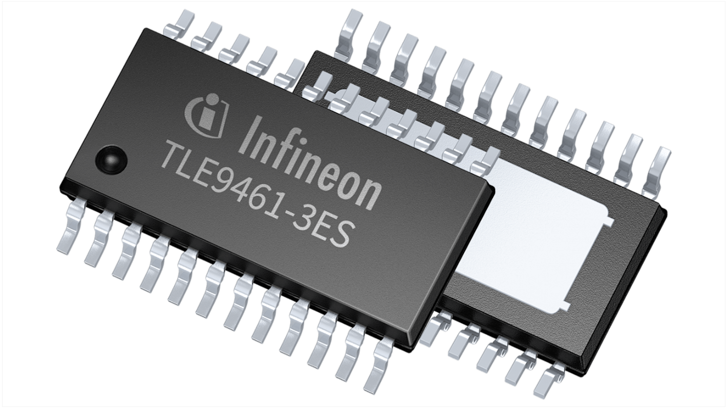
Infineon System-On-Chip, TSDSO-24, für Kfz
- RS Best.-Nr.:
- 244-2898P
- Herst. Teile-Nr.:
- TLE94613ESXUMA1
- Marke:
- Infineon

Mengenrabatt verfügbar
Zwischensumme 20 Stück (auf Gurtabschnitt geliefert)*
CHF.57.12
Auf Lager
- Zusätzlich 2’898 Einheit(en) mit Versand ab 15. Dezember 2025
Sie benötigen mehr? Benötigte Menge eingeben und auf „Lieferverfügbarkeit überprüfen“ klicken.
Stück | Pro Stück |
|---|---|
| 20 - 48 | CHF.2.856 |
| 50 - 98 | CHF.2.688 |
| 100 - 198 | CHF.2.499 |
| 200 + | CHF.2.331 |
*Richtpreis
- RS Best.-Nr.:
- 244-2898P
- Herst. Teile-Nr.:
- TLE94613ESXUMA1
- Marke:
- Infineon
Technische Daten
Mehr Infos und technische Dokumente
Rechtliche Anforderungen
Produktdetails
Finden Sie ähnliche Produkte, indem Sie ein oder mehrere Eigenschaften auswählen.
Alle auswählen | Eigenschaft | Wert |
|---|---|---|
| Marke | Infineon | |
| Anwendung | Kfz | |
| Gehäusegröße | TSDSO-24 | |
| Alle auswählen | ||
|---|---|---|
Marke Infineon | ||
Anwendung Kfz | ||
Gehäusegröße TSDSO-24 | ||
The Infineon TLE94613ESXUMA1 device is designed for various CAN automotive applications as main supply for the microcontroller and as interface for a CAN bus network including the CAN Partial Networking feature. To support these applications, the System Basis Chip (SBC) provides the main functions, such as a 5 V lowdropout voltage regulator (LDO) for e.g. a microcontroller supply, another 5 V low-dropout voltage regulator with off-board protection for e.g. sensor supply, a HS-CAN transceiver supporting CAN FD and CAN Partial Networking (incl. FD tolerant mode) for data transmission, a high-voltage GPIO with embedded protective functions and a 16-bit Serial Peripheral Interface (SPI) to control and monitor the device.
Fully compliant to “Hardware Requirements for LIN, CAN and FlexRay Interfaces in Automotive Applications” Revision 1.3, 2012-05-04
Charge pump-Output for N-channel MOSFET reverse-polarity protection with integrated spread spectrum modulation feature for optimum EMC performance
Universal High-Voltage Wake Input for voltage level monitoring and wake detection
General Purpose High-Voltage In- and Output (GPIO) configurable as Fail Output, Wake Input, Low-Side switch or High-Side switch
HIgh-Voltage Measurement Function as alternate pin assignment
Fail Outputs for Fail-Safe signalization
Configurable wake-up sources
Reset Output & Interrupt Output